Showing posts with label materials. Show all posts

Friday, September 11, 2009

summer recap, part 3.

After my brief stop at the APS, I caught a flight over to Washington, DC, for the fall 2009 ACS national meeting!

panorama of ACS 09 exhibition hall

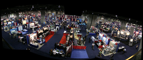
Above: a stitched-together panorama of the ACS exhibition hall. If you have the bandwidths, click here to view it in its large and gloriously full sized glory. I'm not one for free crap, but if you are, let me tell you: you certainly missed out. Silly hats, NASA goody bags, loads of cheap candy: the exhibition had it all.

If the eMRS was a big conference, then the ACS was a colossal one. ACS conferences are very slick and very large, the New York City to my previous conference experiences' New Jersey. My talk being scheduled extremely early on Sunday, the first day of the conference, I was left with basically a whole week to gawk and indulge in some first-rate scientific tourism.

And gawk did I ever! In the interests of time and sanity, I won't recap each and every talk I saw. However, I do want to highlight a talk from Dr. Paul Alivisatos from UC Berkeley.

Dr. Alivisatos, in case you didn't know, was a postdoc with Dr. Louis Brus at AT&T Bell labs, who pioneered the collodial synthesis of II-VI quantum dots and initiated what has become one of the most promising areas of nanoscience.

They've expanded this work to make sophisticated morphologies and sizes, developing knowledge on how size and shape on the nanoscale fundamentally effect the optical and electronic properties of these materials and understanding on how to optimize those properties for a huge range of nanotechnologies. And they glow all purty, to boot.

At the ACS, Dr. Alivisatos presented recent work on the synthesis of heterostructured nanorods [1] that was recently published in JACS (doi: 10.1021/ja809854q).

Heterostructures, as I mentioned sort of in my eMRS post, are a terribly exciting emerging area of materials science, physics and chemistry. You can imagine all kinds of awesome applications which combine the spiffy properties of your favourite materials, particularly in the area of photovoltaics, where such innovation is sorely needed.

The trouble is making the dang things, though. And what the Alivisatos group has done with these rods is a doozy of a synthesis:


As I mentioned above, Alivisatos and others have developed widely-utilized synthetic techniques to prepare size-monodisperse, single crystalline quantum rods and dots using many useful II-IV materials such as CdSe and CdS. You can imagine that it's difficult to talk a nanorod into spontaneously forming a well-defined heterostructure; a common approach is to prepare a regular nanorod and then try to nucleate a second phase onto a certain crystal face which is more reactive to deposition. The nanorods don't always listen to what you ask of them, though, and competing homogeneous nucleation is a pain.

Alivisatos here presents an alternative approach, using cation exchange. There is a thermodynamic drive to exchange Cd2+ ions in CdSe with Ag+ ions to form Ag2Se, for example, of about -1000 kJ/mol.[2] As a heterogeneous reaction in the bulk, this is met with a very large activation energy due to the slow nature of migrating atoms and ions through a solid. Nanoscale materials, however, can overcome this through coordinative unsaturation of surface atoms, changes to more molecule-like kinetics, resulting in a spontaeous displacment under mild, room-temperature and pressure conditions.

This can allow you to synthesize nanorods out of materials that don't necessarily want to form anisotropic structures. For instance, PdS, which it would be very nice to form those nice nanorods using these procedures, has the rocksalt crystal structure, which has centrosymmetric, and does not have a high-energy crystal face that could preferentially nucleate nanorod growth. However, by performing a two-step cation exchange first with CdS rods and Cu+ and then Pb2+, Alivisatos presented that PbS nanorods with the same size and aspect ratio can be prepared. Nifty!

Anyway, back to the main topic at hand: heterostructures! By slowly and carefully adding in a new cation (either Ag+ or Cu+), Alivisatos and coworkers were able to observe that different heterostructures were formed.


They do some fancy modelling and hypothesizing to figure out why:

  • The CdS nanorods have the hexagonal wurzite structure. Interestingly, the c-axis (which extends along the length of the rod) does not have inversion symmetry, meaning that the ends of the rod have different reactivity; Alivisatos states that Cd atoms at one end expose only one dangling bond, whereas the other end exposes three. As well, the sides of the rod are predicted to be much less stable, with an energy cost of formation 7 times that of the tip.
  • The other factor in determining the heterostructure shape is lattice mismatch. Ag2S has a much worse mismatch, leading to increased interfacial strain. This leads to a striped structure.
  • However, Cu2S, which has a monoclinic structure, has an excellent epitaxial match with CdS in the S lattices. Thus, chemical reactivity of different lattice planes dominates the structure formed, leading to Cu2S caps on the end of the nanorods.
  • As well, growth of the Cu ions will occur preferentially at sites where nucleation has already occurred. By controlling the rate of Cu+ addition to the reaction, the Cu2S caps can either be preferentially placed on one or both ends of the rod.
Now, if that isn't the darn tootingest, coolest synthesis of nanomaterials that you've seen in a while, leave a comment with a reference and I'll print out my post and eat it for lunch.

The rest of the talks were also awesome. Also: Tobin Marks looks just a little bit like Woody Allen. A really friggin' smart Woody Allen.

Also! a big shout out to Will from Will and Beyond! I am very confident in reporting that he exists in real life. He was very gracious in showing me a bit that DC has to offer, including some great food in Chinatown and a pirate themed bar in Maryland. Pirates, ho!

Thus concludeth my gigantic summer wrap up. Thanks to anyone that's made it this far through it all. I am angling to try and update this on a regular (weekly?) basis, and have a few ideas kicking around about how to make it easier to do that. Subscribe or comment, and help keep my little pet ego from starving!

[1] A nanorod is a cylindrical nanoparticle, with an aspect ratio around 3-5. Rods are an interesting morphology for numerous applications because the shape can help facilitate things like charge separation.
[2] Alivisatos et al., Science, 2004.

Sunday, February 15, 2009

In which I drink the James Tour Koolaid

As I mentioned last week, James Tour of Rice University gave an invited talk at my university last week (unfortunately, it looks like the abstract is no longer available online).

I was really looking forward to it, as the internets have lots to say about his work, particularly regarding his "nanocars" and other buzzwordy "nano" objects, and on a few of his personal beliefs.

He gave a talk in a pretty packed lecture hall (one of the professors in the department brought his class of undergrads to the talk, which I thought was pretty nifty), and I was also able to ask him some questions afterwards when he met with a group of students for an hour or so.

I was really impressed with a lot of his work, no ifs ands or buts. Contrary to my expectations, his group does a lot of awesome research outside the nanocar dealership, particularly concerning work on carbon nanotubes and graphene.

In particular, he highlighted two areas that were particularly impressive.

Area #1: The Tour group has recently performed some work on the chemical synthesis of graphene:


Graphene is an allotrope of carbon that is simply a sheet[1] of graphite, one atomic layer thick. Think of it as the world's biggest planar aromatic molecule. It has lots and lots of predicted applications as it seems to be incredibly conductive along the sheet.

The main issue is that there really aren't any good ways to make it yet. I kid you not, probably the best way to do so is to pay an undergrad $10 an hour to take a piece of graphite and use Scotch tape to peel off layers until you may or may not get graphene. Yikes.

But, have no fear, because chemistry can come to the rescue! A single-walled carbon nanotube is basically like a sheet of graphene rolled up into a straw. By cleverly oxidizing a nanotube with an oxidizing agent like KMnO4, researchers have shown than you can "un-zip" the nanotube into a sheet of graphene oxide.

What Tour has done that is kind of spiffy is used some diazonium chemistry that his group has helped develop along with a hydrazine reduction to reduce those sheets of graphene oxide back down to functionalized graphene. After, the graphene shows high conductivity along the sheet, indicating that any residual oxygen is not too detrimental to the use of this method for electronic applications. Cool!

Reference: Lomeda, J.R., Doyle, C.D., Kosynkin, D.V., Hwang, W.-F., Tour, J.M. "Diazonium Functionalization of Surfactant-Wrapped Chemically Converted Graphene Sheets." JACS, 2008, 130 (48), pp 16201–16206, DOI: 10.1021/ja806499w

Area #2: As I mentioned above, there's a lot of interest in the electronic properties of graphene as a potential replacement for Si in devices. As well, sensible ways to make graphene are currently few and far between. Or is there?

Researchers have been able for a while to make thin layers of carbon using chemical vapour deposition, called graphitic sheets. Whether or not this constitutes graphene depends on how strict you are at defining these somewhat arbitrary and (decidedly not IUPAC, at least for now) terms[2].

Tour et. al grew thin films of graphitic sheets on "nanocables" of SiO2 (read: thin wires) across two Pt electrodes. Since the SiO2 is an insulator, this means they were able to check the electrical properties of the graphitic sheets wrapped around the wires.

(Above: schematic depicting how they made the nanocables. The squiggly lines in image D correspond to the graphitic thin film)

They observed some very peculiar electronic information, as shown below in figure A. Namely, as they ran through the CV curve, they noted at past a set voltage, the current would rapidly drop off. Furthermore, the switch off seemed extremely reversible, simply requiring the application of a voltage below that what was required to switch it off to turn it back on. The difference between the "off" and "on" states was extremely high, on the order of 10^6 or 7 (figure B). Finally, this switching process was not impacted significantly by the introduction of ambient conditions, nor upon the irradiation of the wires by X-rays.


Now, what is a switch with a very high signal-to-noise ratio good for? Memory applications! Tour attributed the switching process to a "nanoelectromechanical" mechanism whereby the application of a high voltage (erasing the memory) made the wire break (shown below), preventing any current from flowing, and the application of a lower voltage (writing the memory) could heal it back again. Crazy!


This sort of memory device has some nifty advantages over the status quo flash memory ones. In particular, it's a two terminal device that doesn't require a gate; the write/erase voltage is controlled by the size and thickness of the graphitic film. As well, since it is based on a pseudomechanical process (almost like a relay switch), it is resistant to charge interference. Flash memories would be wiped out in the case of an EMP or nuclear explosion, but this (in theory) would be okay. Finally, as I mentioned above, making these sorts of materials by CVD is straightforward, and amenable to industrial-type scale up. Similar two terminal memories exist, based on topics such as phase-change materials, but have been unable to match this extremely high signal to noise ratio.

Reference: Li, Y., Sinitskii, A., Tour, J.M. "Electronic two-terminal bistable graphitic memories." Nature Materials, 2008, 7 (12), pp. 966-971,DOI: 10.1038/nmat2331.


So, in summary: James Tour does some really cool work beyond what you might think! He also presented on some of his nanocar work, of which I am slightly less enthused compared to the above work (he has made several different "nanoautomobiles" including a "nanotruck", a "nanoworm" and a motor-driven nanocar. No word on any "nanobailouts" for the nascent nanoChrysler company- I guess self-assembly machines haven't quite figured out how to unionize yet). I'm just nanokidding! Anyways, enough with the nanopuns. Check out some of Tour's other work!

[1] Graphene is currently defined as anything less than 10 atomic layers of graphite, but as you increase the number of layers, you lose the funky conductivity that makes it so interesting. Hence, the search for a chemical method for large-scale production of single sheet graphene.

[2] Will and Beyond made a great list of some really out-there nano terms. The use of "graphene" to describe carbon-based large aromatics may soon suffer a similar fate. While I was really impressed with almost everything Tour presented on, I somewhat disagree with his overuse of the "nano" prefix, particularly for his nanocars projects. It may get a lot of mainstream media, but it really dilutes what the term can mean, and can induce a lot of eye-rolling from established people in the field.